memristors · eda · layout · knowm-history · ai-hardware
Chapter 3c: The Thermodynamic Bit, Built
Simulate a memristor synapse, draw it polygon by polygon, and send it to the fab — the part of building neuromorphic hardware where a circuit idea becomes silicon.
By Tim Molter ·
When people picture chip design they picture a fab — clean rooms, steppers, robots moving wafers in the dark. They don’t picture someone drawing rectangles. But before any of that happens, somebody has to draw the thing: every electrode, every via, every crosspoint, polygon by polygon, until you have a set of masks. This is the story of one Knowm memristor synapse making that journey — from a circuit you simulate on a laptop, to a layout drawn by hand in Electric, to a real device you can probe on the bench.
The whole stack serves one goal: a pipeline that runs from a machine-learning model all the way down to chip masks, with nothing closed in the middle. Model → masks → chips. That’s why every tool in our stack is open and scriptable — Electric for layout, our own JSpice engine for circuit simulation, and QUCS/Xyce as cross-checks. You can’t automate a pipeline that has a black box in it.
Start with a simulation#
Long before anything gets drawn, you want to know the circuit works. A Knowm synapse is a differential pair (the “2-1” synapse) — two memristors sharing a common node so the pair behaves as one adaptive element. So the first thing we do is build that circuit in simulation, drop in a memristor model, and drive it.
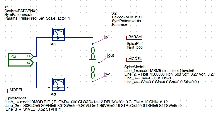
If you want to reproduce this yourself, we’ve written up the Knowm memristor model for several simulators: the M-MSS model in QUCS-S with Xyce, the mean metastable switch model in Xyce, and the models in LTspice.
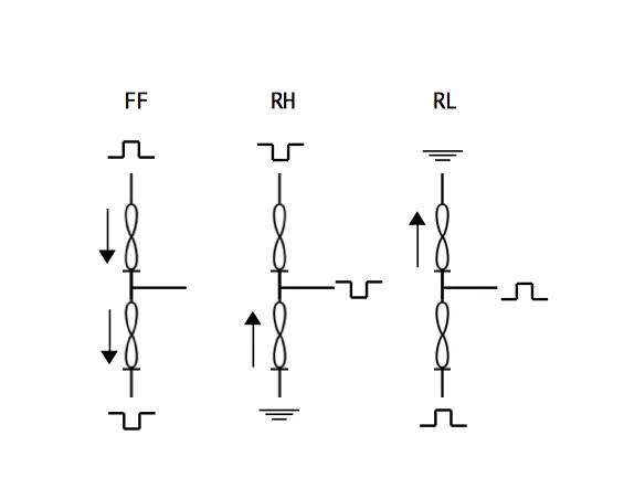
Driving the synapse comes down to a small set of pulse patterns, and they’re worth
keeping in mind because the layout exists to make them possible. Each is a
two-letter code — a forward (F) or reverse (R) drive paired with an operation. The
three you’ll meet first are FF (forward float, the read), RH (reverse high) and
RL (reverse low) — the two writes that push the synapse up toward +1 or down toward
−1. Each is just a pattern of pulses applied across the pair.
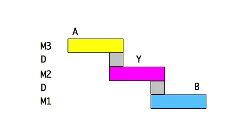
Draw the device: the side view#
Once the circuit checks out, you have to render it as physical layers. The 2-1 synapse is stacked — two memristive junctions sandwiched between three metal layers (M1, M2, M3), so it occupies vertical space, not just area. The cross-section is the clearest way to see what’s being built:
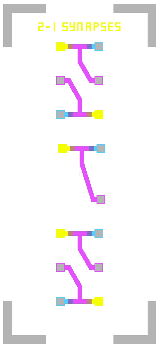
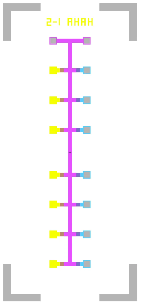
Compose the masks#
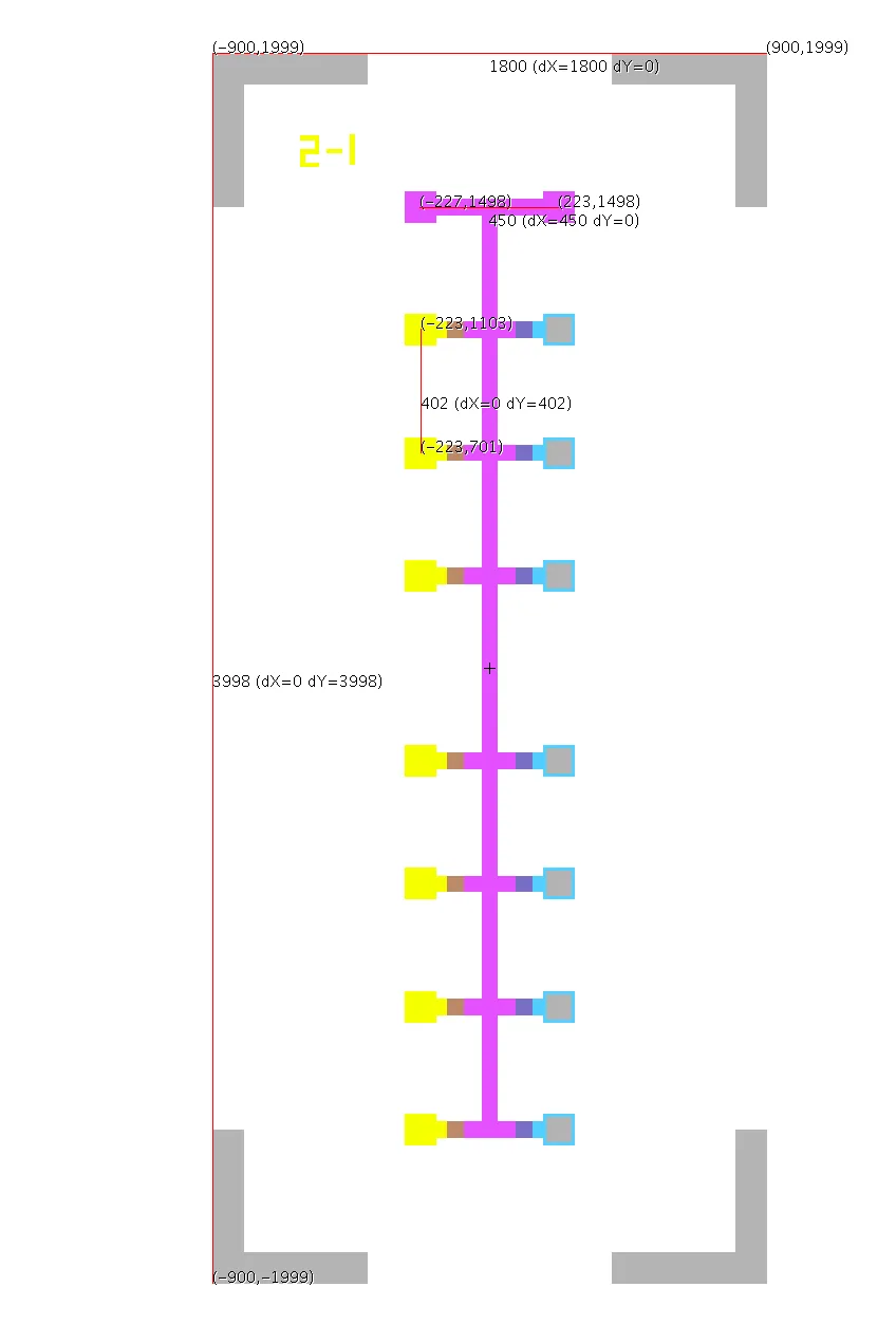
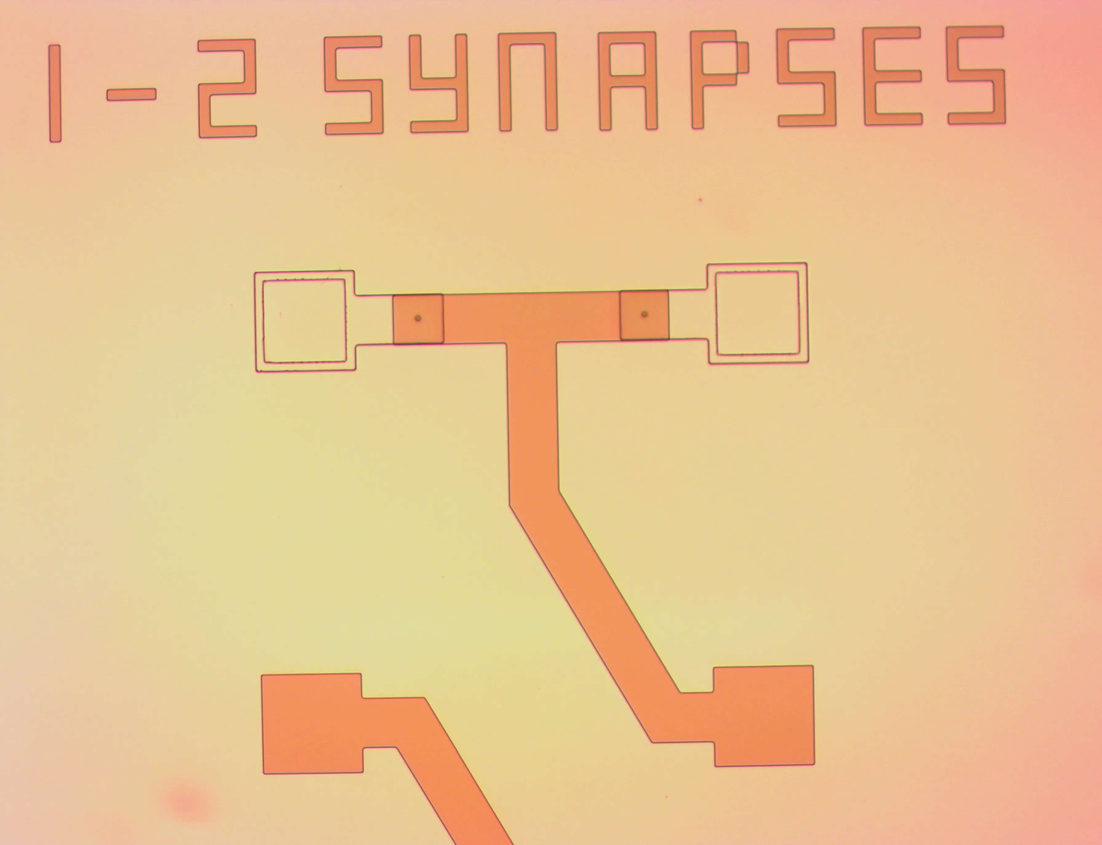
Each of those layers is a separate mask. Overlay them and you get the physical layout — the thing the fab patterns. Here is the 2-1 synapse drawn in Electric: the magenta routing is the shared electrode weaving between the pads, with the device terminals broken out to the pad frame and alignment marks bracketing the corners.
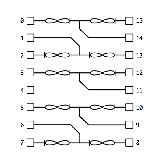
Wire it to the chip#
Zoom out one more level and you have the die itself: sixteen pads, eight per side, with synapses wired between them. This is the chip-level circuit — what each of those 16 bond pads connects to.
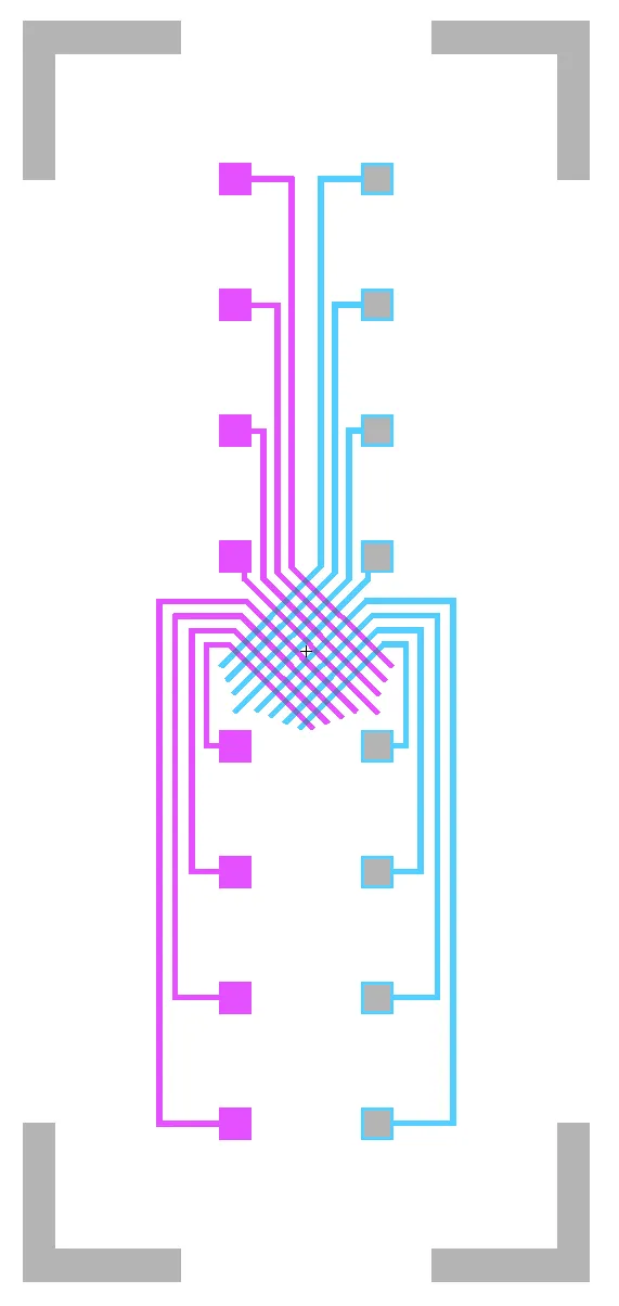
The rest of the family#
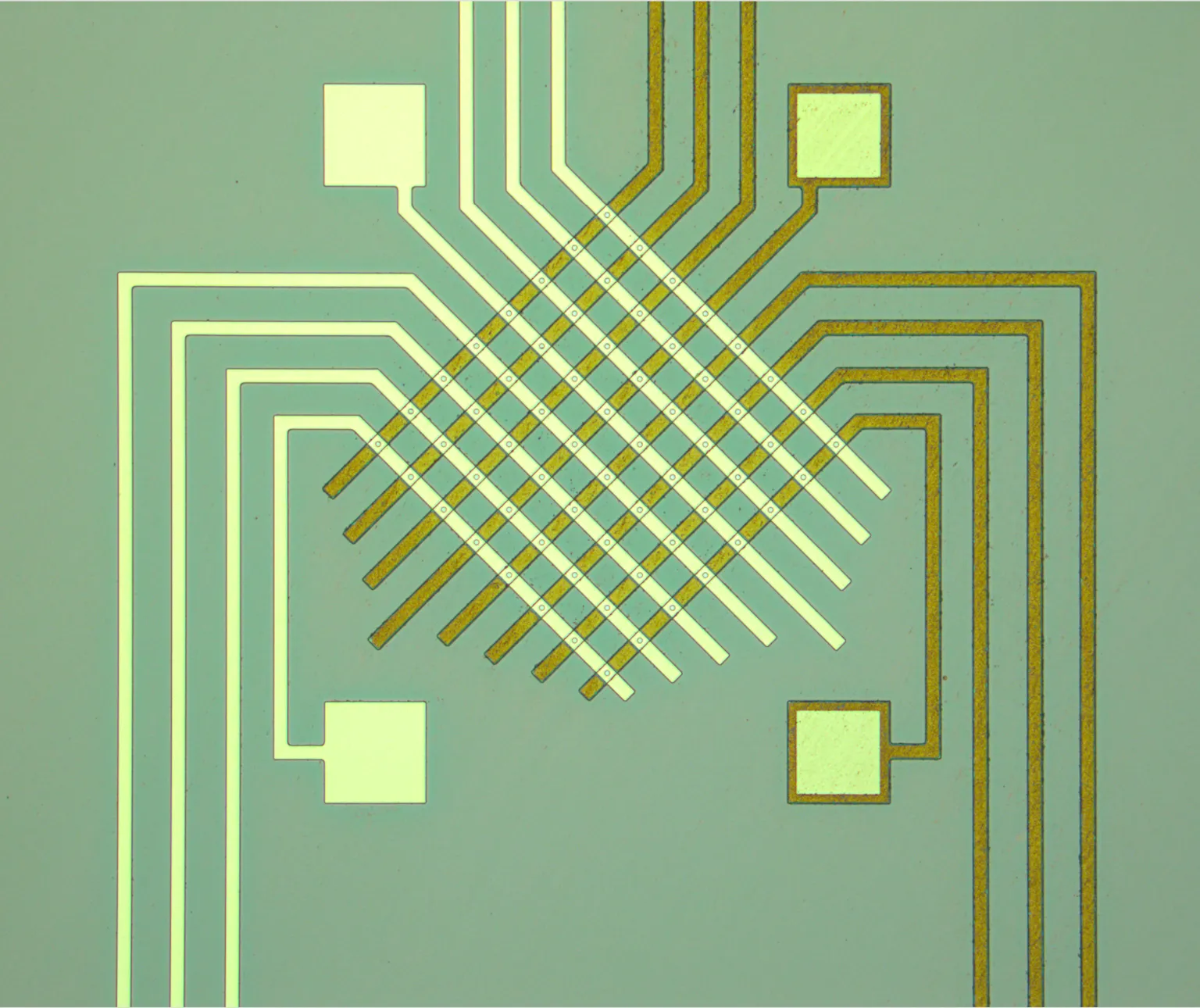
The synapse was the unit cell, but the same approach produced a whole family in Electric — AHaH nodes, OR gates, discrete memristor test structures, and the crossbar. The AHaH node is just synapses ganged onto a shared electrode:
And the crossbar is the one that looks like art: top electrodes running one way, bottom electrodes the other, a memristor at every crossing.
Onto the wafer#
Every design drops into a fixed envelope — each die is 1800 µm × 4000 µm with its sixteen inline pads — and then the die tile across the wafer.
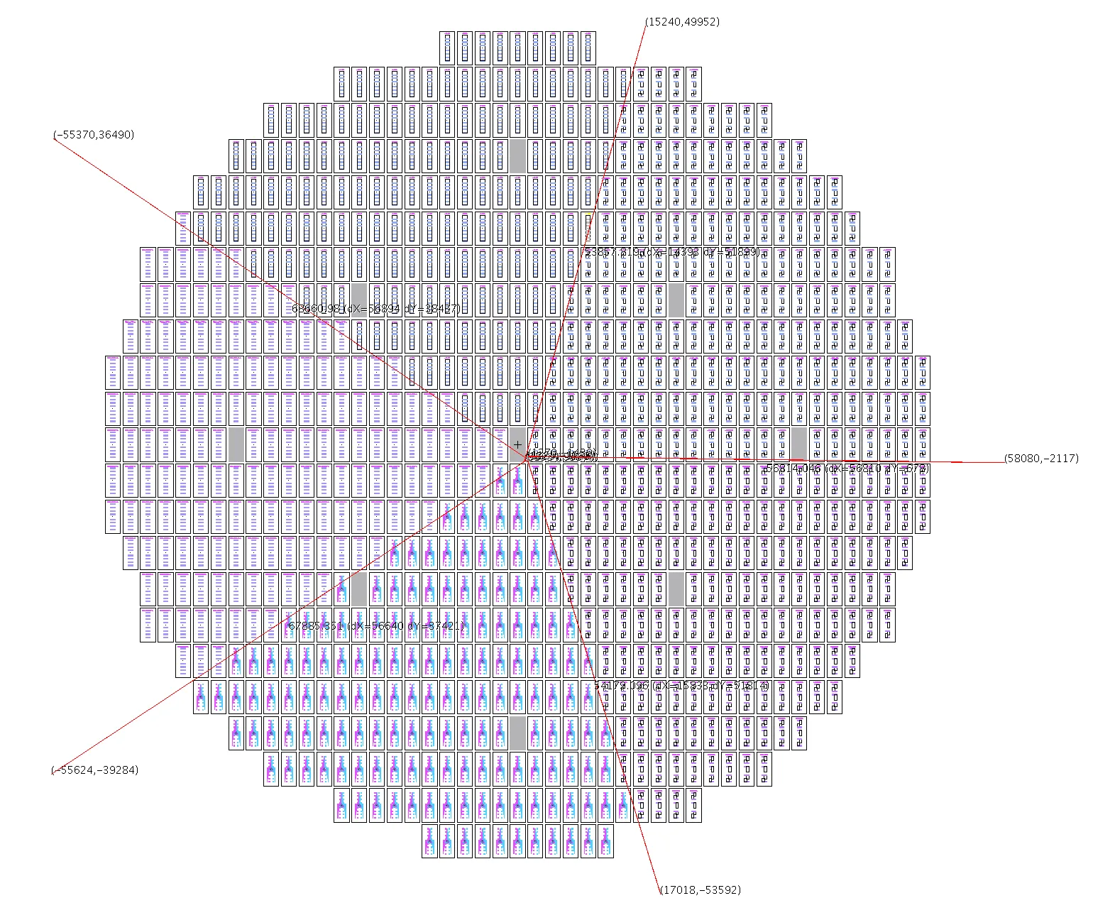
We ended up splitting the run across two wafers: a 3-mask wafer for everything the basic process can already make, and a 5-mask wafer for the stacked 2-1 designs that need extra layers. The devices were fabricated by Dr. Kris Campbell’s lab at Boise State, building on a stacked “double-device” synapse concept she’d developed there. Campbell flagged one real risk: the crossbar’s metal geometry is different enough from everything else that it could etch at a different rate. Her call was low-risk given our large feature sizes — and that’s how it played out: the devices, crossbars included, came out fine on these wafers.
What the fab actually does#
The masks then go to a fab — Dr Kris Campbell’s lab, in our case — and become metal on silicon. It’s a simpler process than the clean-room mystique suggests. It’s the same one behind every chip, and the whole job is pattern transfer: copy the geometry you drew into a physical layer, then repeat for the next mask. Three kinds of equipment do the work.
Deposition lays the film down. Sputtering is closer to sandblasting than painting. The wafer sits in a vacuum chamber facing a slab of source material — the target. Bleed in a little argon, strike a plasma, and the argon ions slam into the target hard enough to knock its atoms loose; the freed atoms drift across the chamber and rain onto the wafer, stacking up into a film a fraction of a micron thick. The metal electrodes go down this way, and so does the memristor material between them, each from its own target without breaking vacuum. The whole stack deposits in one pump-down — a single fast, reliable step, not a separate run per layer.
Lithography prints the pattern. The wafer gets a light-sensitive coating on a spin-coater, the mask is aligned over it, and the pattern is exposed through the mask on a contact aligner — a precision photographic printer for chips. Develop it, and the geometry you drew in Electric now sits in the resist, protecting the film below exactly where you want metal to stay.
Etching carves the rest away. Where the resist isn’t, the film comes off — a reactive plasma for some layers, a beam of ions that physically mills metal for others. Strip the resist and one clean patterned layer is left, and the print-and-etch repeats for each mask in the stack. Between rounds a microscope checks alignment and a profilometer checks film thickness; at the end a probe station tests the devices electrically, and a dicing saw cuts the wafer into individual chips.
None of this needs a leading-edge fab. The features here are large — microns, not nanometers — so a contact aligner, a sputter system, and an etch tool are enough, all standard equipment in cleanrooms and commercial fabs worldwide. The device scales down just as cheaply: the memristor works at nanometer dimensions and stacks on finished CMOS as a back-end-of-line (BEOL) step. The CMOS fab defines the vias with the fine lithography it already runs, and a much cheaper BEOL process then deposits memristor material into those vias and patterns the larger common electrodes on top.
A real device#
Here are two of those designs after fabrication, under the microscope — the same shapes from the Electric layouts, now patterned in metal on a wafer. First the 1-2 synapse:
And the crossbar — the same woven pattern from its Electric layout, now in copper. These exact masks became a shipping part: the 8×8 W-SDC memristor crossbar, packaged in a DIP-16 you can buy and probe.
Driving them on the bench#
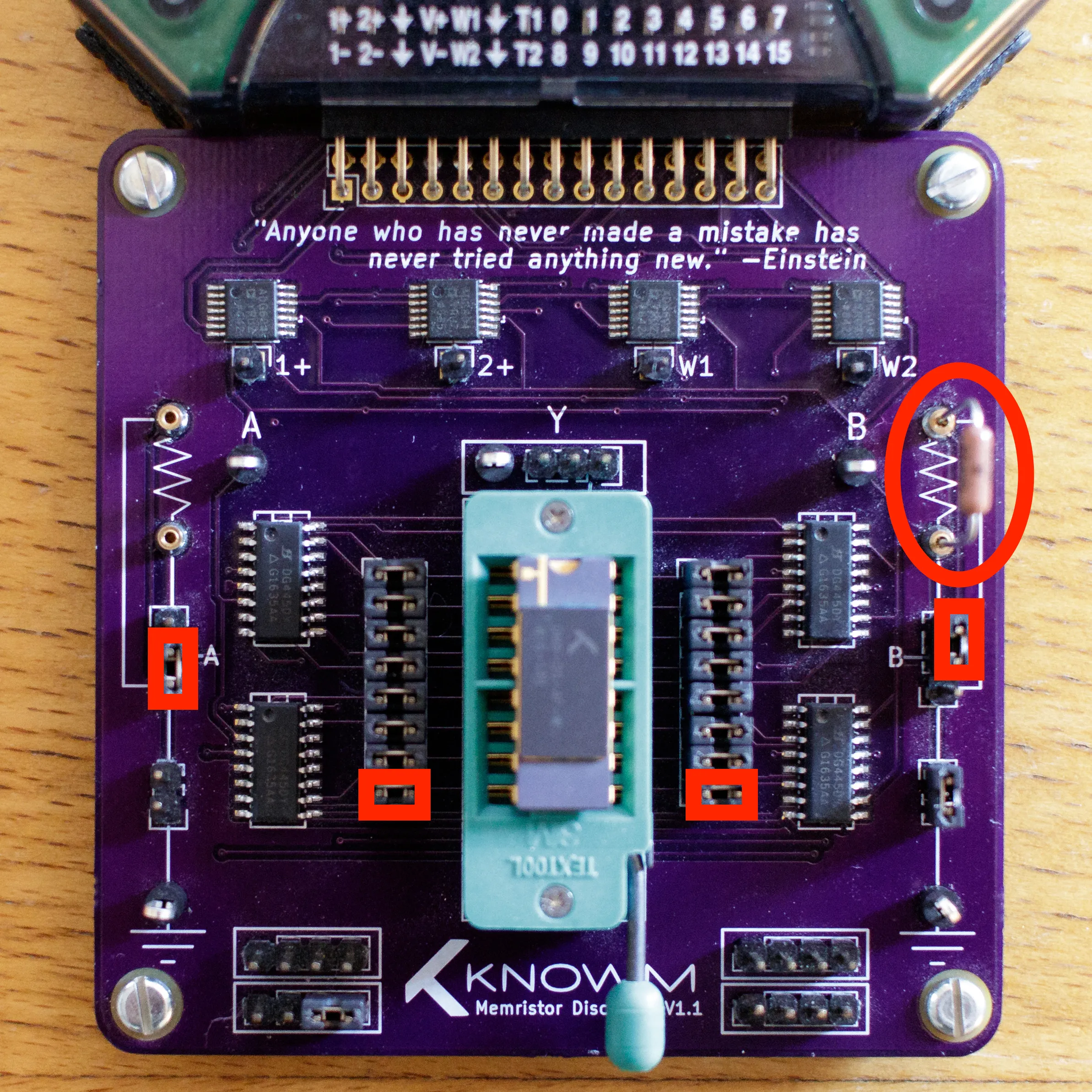
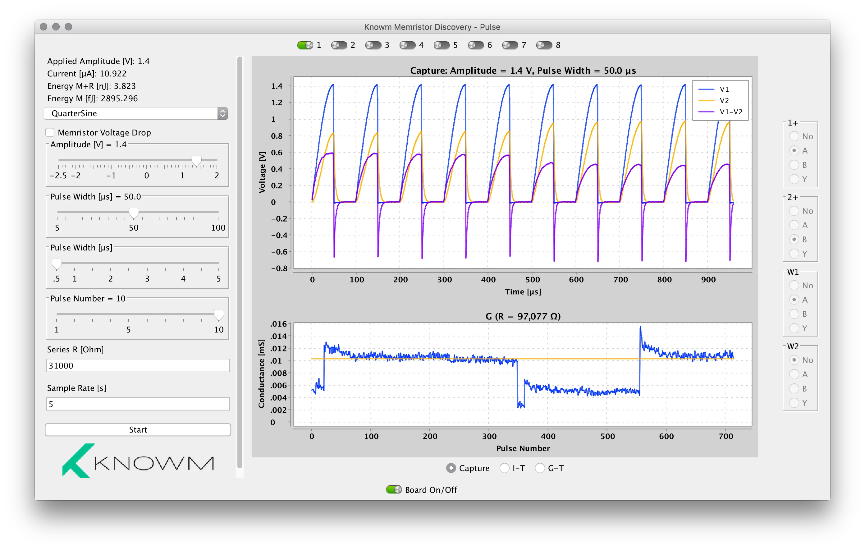
Layouts and wafers are slow, so in parallel we built the Memristor Discovery board to actually drive synapses while the silicon caught up. It routes two waveform generators and two scope channels to any node on the board, switches memristors in and out of the circuit, and generates pulses straight from software — down to 500 ns, with headroom toward 100 ns.
A real synapse, driven by pulses, its conductance stepping as we write and read it:
See it run#
Here’s Alex putting a synapse through its paces on the Memristor Discovery board — writing and reading it live:
Alex demonstrating Knowm synapses in action on the Memristor Discovery board. (Vimeo)
Where it led — and where it stops#
Drawing rectangles in Electric doesn’t feel like building a brain. But this is where the pipeline turns an idea into atoms — the part between a circuit and a physical device — and there’s no shortcut through it. The simulation became a layout, the layout became masks, the masks became a wafer, and the wafer became a device you can hold a probe to.
Step back and look at the whole arc. We started with the memristor itself — got the material and the model right, then paired memristors into kT-bit synapses, wired synapses into neurons, and tiled it into crossbars you can buy and drive on the bench. Years of work, and every layer of it real: a fully open, scriptable path from a model to a mask, and devices at the end of it.